Jul 12, 2026Success Stories
The reasons for the warping of the PCBA board
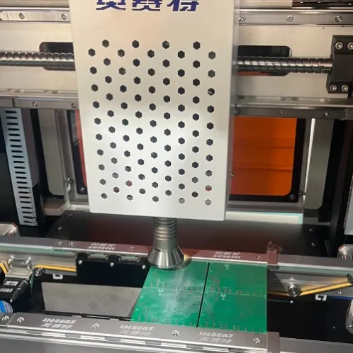
The reasons for the warping of the PCBA board
During the reflow soldering and wave soldering processes, due to various factors, the PCBA board may deform, resulting in poor soldering of the PCBA. This has become a problem that troubles the production staff. Now, let's analyze the reasons for the deformation of the PCBA board.
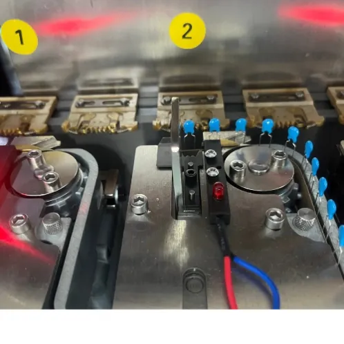
- PCBA board reflow temperature
Each circuit board will have a maximum TG value. When the reflow soldering temperature is too high and exceeds the maximum TG value of the circuit board, it will cause the board to soften and deform.
2. PCB Board
With the popularity of lead-free processes, the temperature of the soldering furnace is higher than that of lead-based ones, and the requirements for the boards have also become increasingly strict. Boards with lower TG values are more prone to deformation during the soldering process, but higher TG values result in higher prices.
3. Thickness of PCBA board
As electronic products continue to evolve towards smaller and thinner designs, the thickness of circuit boards is also increasingly striving for reduction. The thinner the circuit board is, the more susceptible it is to deformation when exposed to high temperatures during reflow soldering.
4. Size of PCBA board and number of panels
When the circuit board undergoes reflow soldering, it is generally transported on a chain. The chains on both sides serve as support points. If the size of the circuit board is too large or the number of panels is excessive, the circuit board is prone to sink towards the center point, resulting in deformation.
5. The depth of V-Cut
V-Cut will damage the structure of the board. V-Cut cuts grooves on the original large sheet of material. If the V-Cut line is too deep, it will cause deformation of the PCBA board.
6. Uneven copper coverage on the PCBA board
Most circuit boards are designed with large areas of copper foil for grounding purposes. Sometimes, the Vcc layer also has large areas of copper foil. When these large areas of copper foil cannot be evenly distributed on the same circuit board, it will cause uneven heat absorption and heat dissipation speeds. The circuit board will naturally expand and contract, and if the expansion and contraction cannot occur simultaneously, different stresses will be generated and the board will deform. At this time, if the temperature of the board has reached the upper limit of the TG value, the board will start to soften and undergo permanent deformation.
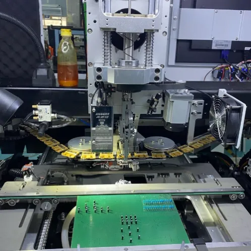
7. Connection points on each layer of the PCBA board
Today's circuit boards are mostly multi-layer boards, with many drilled connection points inside. These connection points are classified as through holes, blind holes, and buried holes. These connection points can limit the effect of thermal expansion and contraction of the circuit board, thereby causing the board to deform.