Jul 19, 2026Services Overview
The role of plasma cleaning machine in SMT process: why high-end electronic manufacturing cannot do without it?
In high reliability SMT production scenarios such as automotive electronics, semiconductor packaging, and medical electronics, virtual soldering
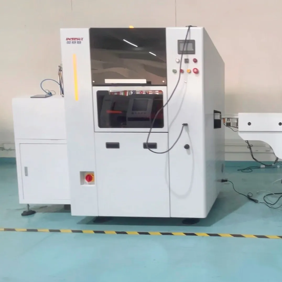
The role of plasma cleaning machine in SMT process: why high-end electronic manufacturing cannot do without it?
In high reliability SMT production scenarios such as automotive electronics, semiconductor packaging, and medical electronics, virtual soldering, coating peeling, and bonding failure are the core pain points that have a long-term impact on product yield. Most of these failure issues stem from micro pollution on PCB pads and component surfaces that is not visible to the naked eye, including residual organic oil stains, oxide layers, flux residues, and micron sized dust from processing. Traditional wet cleaning is difficult to completely remove such micro pollutants and can easily cause chemical residues and device damage. Atmospheric pressure plasma cleaning technology, with its advantages of non-destructive, efficient, and environmentally friendly, is gradually becoming a standard process for high-end SMT production lines.
Many people's understanding of plasma cleaning is limited to "surface cleaning", but in reality, it plays a dual role in both cleaning and surface activation in SMT processes. Its working principle is to generate a highly active plasma containing ions, electrons, and free radicals through high-pressure ionization process gas. On the one hand, it physically bombards and peels off the surface dust and oxide layer, and on the other hand, it decomposes organic pollutants through chemical reactions, ultimately producing harmless substances such as carbon dioxide and water vapor. The entire process is a dry process, without the need for chemical agents. The processing temperature is usually below 50 ℃, and there is no risk of thermal damage or corrosion to heat sensitive devices and precision PCBs.
In the entire SMT process, plasma cleaning is mainly applied to three key processes, which directly determine the welding reliability and long-term stability of the product. The first step is to clean the solder pads before reflow soldering. During the storage and transportation of PCBs, the solder pads are prone to oxidation and adsorption of organic pollutants, leading to a decrease in solder wettability and the occurrence of defects such as virtual soldering, false soldering, standing monuments, and solder beads. After plasma treatment, the oxide layer on the surface of the solder pad is completely removed, and the surface energy is significantly improved. The solder spreading area can be increased by more than 30%, and the welding yield and solder strength are greatly improved, especially suitable for products with high reliability requirements such as automotive electronics and security electronics.
Next is the pre-treatment process of three proof coating and bottom filling glue. Organic pollution on the surface of PCB can reduce the adhesion between glue and board, leading to blistering, delamination, and peeling of the three proof paint coating, gaps in the bottom filling glue, and ultimately losing its protective effect. Plasma cleaning can activate surface molecules, greatly improve the wetting and adhesion of adhesives, avoid coating peeling and delamination problems, enhance the product's moisture resistance, salt spray resistance, and vibration resistance, and extend the service life of outdoor and industrial grade products.
The third is the pre-processing of semiconductor packaging and COB bonding. In chip packaging and gold/copper wire bonding processes, trace contamination of the chip surface and substrate can directly lead to insufficient bonding strength, resulting in debonding and failure problems. Plasma cleaning can completely remove surface micro pollution without damaging the chip, increase bonding strength by more than 30%, and significantly reduce the risk of packaging failure. It is an essential process for high-end semiconductor packaging and precision optoelectronic device production.
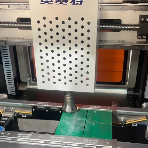
There are two core criteria for selecting plasma cleaning equipment for SMT production lines.
One is to adapt to the production mode. For large-scale continuous mass production, online plasma cleaning machines are preferred, which can be directly connected to the SMT production line and achieve SMEMA communication linkage with the front and rear equipment without additional manual operation; For small batches with multiple varieties and R&D trial production scenarios, offline equipment can be selected for higher flexibility.
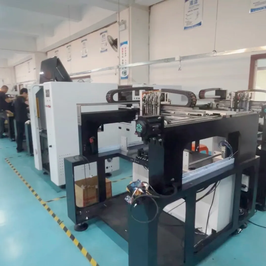
Secondly, attention should be paid to the uniformity and controllability of the process. The uniformity of the whole board processing of high-quality equipment should be ≥ 95%. At the same time, it supports digital adjustment of plasma power, transmission speed, and gas flow rate, and can store multiple sets of process formulas to adapt to PCBs and components of different materials.
With the continuous development of electronic devices towards miniaturization and high reliability, plasma cleaning has gradually become a standard configuration for high-end SMT production from an optional upgrade process. Achieving significant improvements in product yield and reliability at extremely low operating costs is an important process upgrade path for electronic manufacturing enterprises to strengthen product competitiveness and break through the high-end market.